Introduction, The Post-FinFET Era
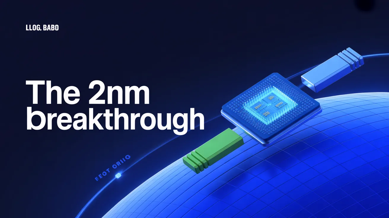
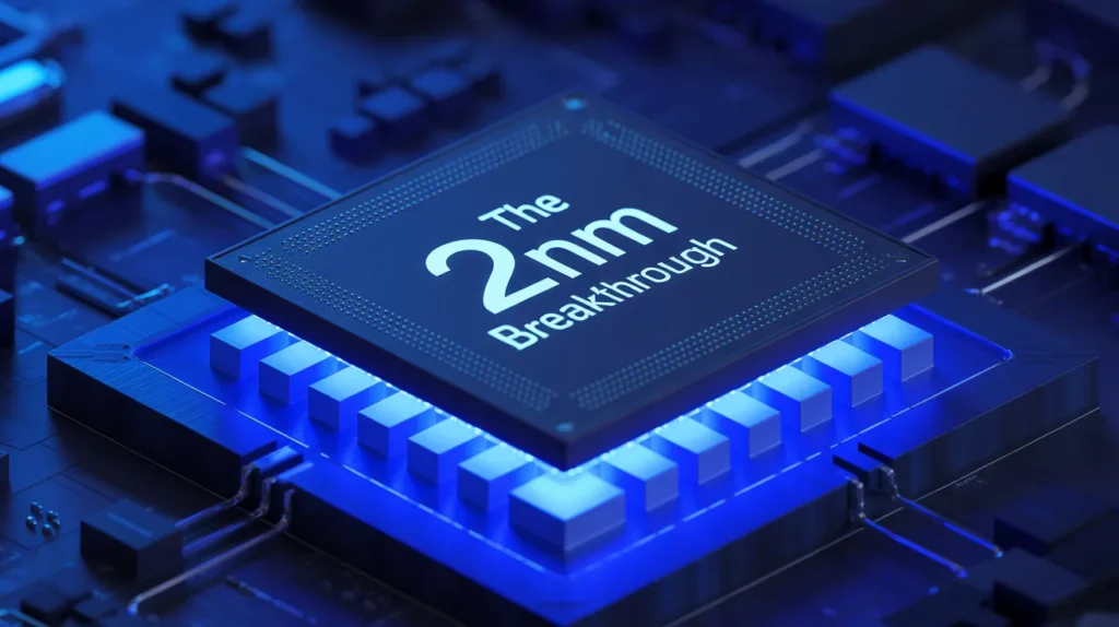
For nearly a decade, the semiconductor industry lived inside the shadow of FinFET scaling. From 16nm through 3nm, FinFET transistors carried Moore’s Law forward with incremental geometry improvements, tighter pitches, and aggressive power optimizations. Yet at Ninth Post, we have been tracking the limits of this architecture for years, and by the early 2020s the physics had become unavoidable. FinFET was approaching a wall. The 2nm Breakthrough: What the Latest Chip Architecture Means for Local AI Inference.
The 3nm generation, delivered by players like TSMC and Samsung Electronics, represented an impressive engineering feat, but it was also a transitional node. Leakage currents were rising. Gate control over increasingly thin channels was weakening. Power delivery networks were consuming too much routing area. Meanwhile, the computing workloads of the modern era, especially AI inference, were expanding faster than transistor scaling.
By 2026, the industry has arrived at what many engineers now call the Angstrom era. Instead of simply shrinking planar dimensions, chip designers are fundamentally redesigning transistor geometry and power distribution.
This is where the 2nm node emerges as the real inflection point.
At Ninth Post, we view 2nm architectures such as TSMC N2 and Intel 18A not merely as smaller process nodes but as the first designs purpose-built for the AI age. Two foundational innovations define this generation:
- Gate-All-Around Nanosheet transistors
- Backside Power Delivery networks
Combined, these technologies allow chips to sustain higher transistor density while dramatically improving energy efficiency.
Why does this matter?
Because local AI inference, especially running compact language models directly on personal devices, has reached a point where hardware capabilities are finally catching up to algorithmic ambition.
The result is a shift from cloud-dependent AI toward privacy-preserving, on-device intelligence.
Table of Contents
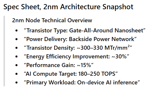
The Physics of 2nm, GAAFET vs. FinFET
The most important architectural change at the 2nm node is the transition from FinFET to the Gate-All-Around Nanosheet transistor.
FinFETs introduced a three-dimensional structure where the gate wrapped around three sides of a vertical silicon fin. This improved electrostatic control compared with planar transistors and allowed scaling down to around the 5nm generation.
But as channel widths approached a few nanometers, three-sided gate control was no longer enough.
Enter Gate-All-Around Nanosheet transistors.
Why Gate-All-Around Matters
In a Gate-All-Around Nanosheet design, the transistor channel is no longer a vertical fin. Instead, it becomes a set of horizontally stacked silicon sheets, each completely surrounded by gate material.
This architecture enables the gate to control the channel from all four sides.
The benefits are significant:
- Superior electrostatic control, reducing leakage current
- Lower threshold voltage variability
- Better scalability below 3nm
- Improved drive current per transistor
In practice, this means chip designers can increase transistor density while maintaining stable power consumption.
At Ninth Post, we often describe this transition as moving from “controlling a riverbank” to “controlling the entire river.”
With FinFETs, electrons could still leak around poorly controlled edges. With Gate-All-Around Nanosheets, the gate surrounds the channel like a sleeve, drastically reducing leakage pathways.
Atomic-Scale Surface Engineering
The physics improvements do not stop at transistor geometry. The Angstrom era is also about surface precision at the atomic level.
Manufacturing equipment from Applied Materials and ASML now operates at resolutions where a few atoms of surface roughness can affect electron mobility.
One of the most notable developments is Applied Materials’ Viva platform, which enables ultra-precise atomic layer smoothing during deposition.
Why does this matter?
Electron mobility inside nanosheet channels is extremely sensitive to surface defects. Even minor roughness can scatter electrons and reduce current flow.
By smoothing the channel at near-atomic precision, these new processes improve:
- Carrier mobility
- Drive current
- Energy efficiency
In other words, the performance gains of 2nm nodes are not just about shrinking transistors. They are about building cleaner ones.
Backside Power Delivery, The Hidden Revolution
If nanosheets represent the visible breakthrough of the 2nm era, power delivery redesign is the hidden revolution.
Traditional chips deliver power through the same metal layers used for signal routing. This architecture is known as frontside power delivery.
The problem is simple. As transistor density increases, routing congestion becomes a major bottleneck.
Power lines compete with signal lines.
The result is voltage droop, noise, and reduced performance.
The Rise of the Backside Power Network
To solve this issue, both Intel and TSMC have introduced backside power delivery systems.
Two implementations dominate the industry:
- Intel’s PowerVia
- TSMC’s Super Power Rail
These technologies move power distribution to the backside of the wafer, separating power and signal routing entirely.
This architecture enables what engineers call a Backside Power Network, where electrical current flows through dedicated vertical vias directly beneath the transistor layer.
The advantages are substantial:
- Reduced IR voltage drop
- Lower power noise
- More routing space for logic
- Higher transistor density
From a systems perspective, backside power is as transformative as the shift from planar transistors to FinFET.
It fundamentally restructures how electricity flows through modern silicon.
The Legacy Bottleneck
Before backside power delivery, chip designers faced several limitations:
- Power rails consumed valuable routing layers
- Voltage droop limited peak clock speeds
- Signal congestion reduced layout efficiency
With Backside Power Networks, these issues largely disappear.
Logic designers gain additional routing capacity on the front side, enabling:
- Larger AI accelerators
- More complex NPUs
- Higher bandwidth memory interconnects
This is one of the key reasons 2nm chips are particularly suited for AI workloads.
Local AI Inference, The 180 TOPS Threshold
The next question is obvious.
What do these transistor improvements mean for actual computing workloads?
The answer lies in AI inference performance per watt.
By 2026, a new metric has become central to mobile and edge AI computing:
TOPS per watt (Tera Operations Per Second per Watt).
For real-time AI workloads such as language models, computer vision, and agentic automation, engineers now estimate that around 180 TOPS of AI compute is required to run modern on-device models efficiently.
This is the point where latency falls below roughly 50 milliseconds, making interactions feel instantaneous.
2nm architectures make this possible.
Next-gen NPU Architecture
Companies like Apple Inc., Intel, and Qualcomm are already building Next-gen NPU Architecture designs optimized for this threshold.
Early benchmarks from prototype chips suggest:
- 200–250 TOPS AI throughput
- 30% energy efficiency gains
- sub-50ms inference latency
This enables devices to run 7-billion parameter language models locally, without constant cloud connectivity.
At Ninth Post, we see this as the beginning of a new paradigm:
On-device AI inference becomes the default computing model.
The Rise of Small Language Models (SLMs)
Large cloud models will still exist, but the next phase of AI computing is defined by Small Language Models.
SLMs are optimized for:
- lower memory footprints
- faster inference
- edge deployment
Examples include:
- 3B to 7B parameter conversational models
- task-specific reasoning models
- local multimodal assistants
The key advantage is latency.
Instead of waiting hundreds of milliseconds for a cloud response, devices equipped with 2nm NPUs can respond almost instantly.
Comparative Analysis, The 2nm Showdown
The race toward the 2nm node is dominated by three major foundries.
Below is a comparative snapshot of their architectures.
| Foundry | Process Node | Transistor Density (MTr/mm²) | Power Reduction | Performance Gain | Key Innovation |
|---|---|---|---|---|---|
| TSMC | N2 | ~330 | 25–30% | 10–15% | Gate-All-Around Nanosheet |
| Intel | 18A | ~300 | 30% | 15–20% | Backside PowerVia |
| Samsung | SF2 | ~290 | 25% | 12% | Early GAA implementation |
While the numbers vary slightly depending on design libraries and chip layouts, the key takeaway is clear.
The 2nm node is not defined by a single innovation.
It is the combination of:
- nanosheet transistors
- backside power networks
- AI-optimized architectures
Together, these technologies enable the next generation of computing platforms.
Theoretical Add-On, The Energy Wall Paradox
Despite the impressive improvements of the 2nm node, a deeper challenge remains.
We call it the Energy Wall Paradox.
The paradox is simple.
Every new process node improves energy efficiency, but computing workloads expand even faster.
For example:
- 2nm chips may deliver 30% better efficiency
- Agentic AI workloads are growing 50% more demanding
This means that while chips are getting better, the energy demand of AI systems continues to grow.
The risk is that hardware improvements merely delay the inevitable energy wall.
In practical terms, this means several trends are emerging:
- Specialized AI accelerators
- model compression techniques
- hardware-aware AI training
The future of AI will not be defined solely by transistor scaling.
It will depend equally on algorithmic efficiency.
The Manufacturing War
Technology breakthroughs mean little without manufacturing scale.
And this is where the semiconductor industry becomes a geopolitical competition.
The 2nm node requires:
- extreme ultraviolet lithography
- advanced packaging
- atomic-level process control
Only a few companies can manufacture these chips at scale.
Today, the two leaders are:
- TSMC
- Intel
Yield Thresholds
For a new node to become commercially viable, yields must reach roughly 60 percent.
Early reports suggest:
- Intel 18A is approaching this threshold
- TSMC N2 has already secured major capacity bookings
One company in particular has moved aggressively.
Apple.
Industry sources indicate that Apple has secured nearly half of the initial 2nm wafer supply.
Why?
Because the company plans to deploy 2nm chips across:
- Mac processors
- iPhone SoCs
- AI accelerators
This strategy ensures that Apple’s ecosystem remains vertically integrated, with hardware optimized specifically for local AI workloads.
The Ninth Post Verdict
At Ninth Post, we view the 2nm transition as the true beginning of the AI-native computing era.
For years, artificial intelligence depended heavily on centralized cloud infrastructure.
That model is beginning to break.
With Gate-All-Around Nanosheets, Backside Power Networks, and Next-gen NPU Architecture, personal devices are gaining enough compute to run sophisticated models locally.
This changes everything.
Privacy improves because data no longer needs to leave the device.
Latency disappears because inference happens instantly.
And developers gain the ability to build AI-first applications that run anywhere.
In practical terms, the 2nm node marks the beginning of a new computing philosophy.
The cloud becomes optional.
The device becomes intelligent.
And for the first time in decades, the most important AI breakthroughs may not happen inside massive data centers.
They may happen directly in the silicon inside our pockets.
Architectural Co-Design, When Silicon Meets AI Models
Another important shift enabled by the 2nm node is the emergence of hardware–model co-design. For most of the computing era, software adapted itself to general-purpose processors. CPUs were built first, and applications optimized later. But AI workloads have reversed this relationship.
Modern AI systems, particularly language models and agent-based reasoning frameworks, place unique stress patterns on silicon. They demand massive matrix multiplication throughput, high memory bandwidth, and extremely low latency data movement. As a result, chip architects are now designing silicon specifically for these computational patterns.
At Ninth Post, we see the Next-gen NPU Architecture emerging as a direct consequence of this shift. Instead of relying on GPUs alone, modern SoCs integrate specialized AI engines optimized for transformer inference. These NPUs include systolic arrays, tensor cores, and ultra-fast SRAM buffers located physically close to compute units.
The 2nm generation dramatically amplifies the impact of these designs. With increased transistor density, engineers can place significantly larger AI acceleration blocks inside mobile processors. This allows developers to deploy transformer-based inference pipelines locally without relying on remote cloud GPUs. In effect, AI workloads are becoming first-class citizens in chip design, rather than secondary accelerators attached to CPU architectures.
Memory Bandwidth, The Silent Constraint of AI Inference
While transistor density often receives the most attention, one of the most critical constraints for On-device AI Inference is memory bandwidth. Language models are not purely compute-bound workloads. They are also extremely dependent on the speed at which parameters and activations can move between memory and compute units.
Even a relatively compact 7-billion parameter model requires several gigabytes of memory bandwidth during inference. If memory subsystems cannot keep pace with compute throughput, the entire AI pipeline becomes bottlenecked.
This is why the 2nm generation is closely tied to advances in memory architecture.
Several techniques are being deployed simultaneously:
- Larger on-chip SRAM buffers to store frequently accessed model weights
- Advanced packaging technologies such as chiplet interconnects
- Higher-bandwidth LPDDR memory subsystems
- AI-specific cache hierarchies optimized for tensor workloads
These improvements allow Next-gen NPUs to sustain high inference throughput without repeatedly accessing slower off-chip memory. The result is not just faster AI responses but dramatically improved energy efficiency.
In practical terms, reducing memory traffic often saves more energy than improving compute efficiency alone. This is one of the reasons why 2nm chips achieve such dramatic gains in TOPS-per-watt performance.
Thermal Density and Power Efficiency
Another major engineering challenge in advanced nodes is thermal density. As transistor counts increase, heat becomes a critical limiting factor. Packing hundreds of millions of transistors into a square millimeter creates localized thermal hotspots that can degrade performance and reliability.
The Backside Power Network architecture indirectly helps solve this issue. By separating power routing from signal layers, designers can reduce resistive losses and lower overall heat generation. Additionally, improved power delivery allows chips to operate at lower voltages while maintaining stable performance.
Lower voltage operation has a compounding benefit. Because dynamic power consumption scales roughly with the square of voltage, even modest voltage reductions can produce significant energy savings.
For AI workloads, this translates into longer sustained inference sessions without thermal throttling. Devices equipped with 2nm chips can maintain high AI throughput without overheating, which is essential for applications such as continuous speech processing, computer vision, and autonomous agents.
Edge Computing and the Collapse of Latency
One of the most transformative implications of On-device AI Inference is the collapse of network latency as a design constraint.
In cloud-based AI architectures, every interaction requires a round trip between the user device and remote data centers. Even with high-speed networks, this introduces unavoidable delays ranging from tens to hundreds of milliseconds.
For conversational interfaces and real-time decision systems, this latency can significantly degrade the user experience.
The 2nm node changes this dynamic by enabling sophisticated AI workloads directly on edge devices. When inference occurs locally, response times drop dramatically because there is no need for network communication.
This creates entirely new categories of applications:
- Real-time translation without internet connectivity
- Personal AI assistants operating entirely offline
- Localized healthcare diagnostics on portable devices
- Autonomous robotics with instant decision loops
In each of these cases, the elimination of network latency fundamentally changes how software systems are designed.
At Ninth Post, we often describe this transition as the migration of intelligence from the cloud to the edge.
Security and the Privacy-First AI Movement
The rise of On-device AI Inference also carries profound implications for data security and privacy. Cloud-based AI systems require users to transmit sensitive data, including voice recordings, personal messages, and behavioral patterns, to remote servers for processing.
This model raises serious concerns about surveillance, data ownership, and regulatory compliance.
Local inference provides a fundamentally different architecture. When models run directly on the device, user data never leaves the hardware boundary. Sensitive information can be processed entirely within secure enclaves embedded in the processor.
The 2nm node makes this approach feasible at scale because it delivers the performance required to run modern models without relying on remote infrastructure.
This is particularly relevant for industries such as healthcare, finance, and government services, where strict privacy requirements often limit the adoption of cloud-based AI systems.
As a result, we are witnessing the rise of what many analysts now call the privacy-first AI movement, where intelligence is embedded directly into consumer devices rather than centralized in hyperscale data centers.
Software Ecosystems Adapting to the 2nm Era
Hardware innovation alone does not create technological revolutions. Software ecosystems must evolve alongside silicon architectures to fully unlock their potential.
Developers are already adapting their frameworks to take advantage of Next-gen NPU Architecture and Gate-All-Around Nanosheet efficiency improvements. Machine learning toolkits are being redesigned to optimize inference pipelines specifically for edge hardware.
Several key changes are emerging in AI software design:
- Model quantization techniques reducing parameter precision
- Sparse neural network architectures that minimize compute overhead
- Compiler optimizations targeting dedicated AI accelerators
- Hybrid pipelines combining CPU, GPU, and NPU execution paths
These techniques allow even relatively small models to deliver surprisingly powerful capabilities when deployed on optimized hardware.
In many cases, software efficiency improvements amplify the gains delivered by the 2nm node, resulting in exponential improvements in real-world performance.
Packaging Innovation and the Chiplet Future
Beyond transistor design and power delivery, advanced semiconductor nodes are also driving innovations in chip packaging. Traditional monolithic chips are becoming increasingly difficult to manufacture as die sizes grow larger and defect probabilities increase.
To address this challenge, manufacturers are increasingly adopting chiplet architectures, where multiple smaller dies are connected through high-speed interconnects within a single package.
This approach provides several advantages:
- Higher manufacturing yields
- Greater design flexibility
- Improved scalability for specialized accelerators
For AI workloads, chiplets enable designers to combine CPU cores, GPU clusters, and dedicated NPUs into modular architectures optimized for specific applications.
The 2nm generation is particularly well suited for chiplet integration because its power efficiency allows more compute units to be placed within a given thermal envelope.
Over time, this may lead to highly customizable processors where AI acceleration blocks can be tailored to specific workloads such as robotics, augmented reality, or large language model inference.
The Long-Term Implications for Moore’s Law
The semiconductor industry has long been guided by the principle of Moore’s Law, which predicts that transistor density roughly doubles every two years. However, maintaining this pace has become increasingly difficult as manufacturing approaches atomic-scale limits.
The 2nm node demonstrates that Moore’s Law is not ending, but it is evolving.
Instead of relying purely on geometric scaling, progress now depends on a combination of innovations:
- Gate-All-Around Nanosheet transistor design
- Backside Power Network architecture
- Advanced packaging and chiplet integration
- AI-specific hardware accelerators
Together, these technologies represent a new phase of semiconductor engineering where architectural creativity becomes as important as lithographic precision.
At Ninth Post, we believe this hybrid approach will define the next decade of computing innovation. The future of silicon will not be determined solely by how small transistors can become, but by how intelligently they are organized to support emerging workloads.
And in the age of artificial intelligence, those workloads are evolving faster than ever before.
Also Read: “RAG vs Graph-RAG: Which Knowledge Retrieval Strategy Actually Wins in 2026?“
FAQs
What is the 2nm node in semiconductor technology?
The 2nm node refers to the next generation of semiconductor manufacturing processes using Gate-All-Around Nanosheet transistors and advanced lithography techniques to increase transistor density and energy efficiency.
Why is 2nm important for AI chips?
2nm chips significantly improve TOPS-per-watt efficiency, enabling devices to run AI models locally with lower latency and reduced power consumption.
What is backside power delivery in modern chips?
Backside power delivery systems like Intel’s PowerVia move power routing to the back of the wafer, reducing voltage droop and freeing frontside routing layers for logic and signal interconnects.